
 Home /
IoT Electronic Product Development: Antenna and Enclosure Co-Design


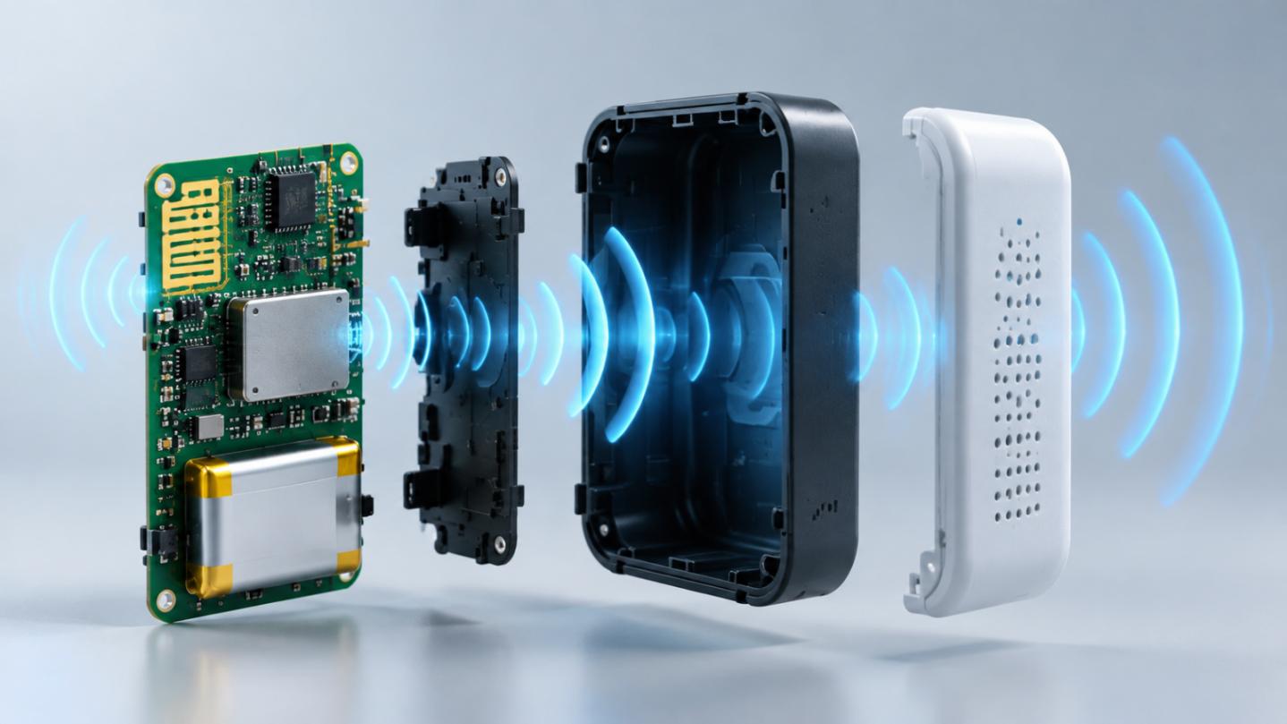

In IoT Electronic Product Development, enclosure geometry becomes part of the RF design. A battery moved closer to the antenna, a conductive coating, or a metal mounting bracket can change wireless performance after the electronics appear complete.
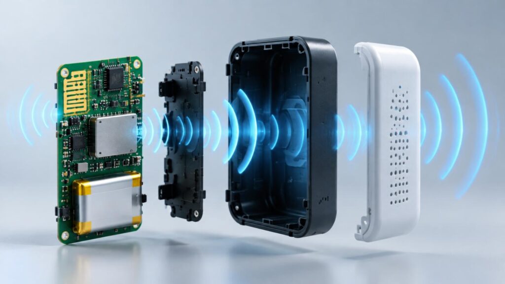
At LKK Design, our services connect industrial design, PCB development, antenna design, RF debugging, DFM, and production support. For antenna–enclosure integration, these disciplines need shared mechanical constraints and measurable acceptance criteria.
1. Perform Range Loss Diagnosis Before Changing Antenna
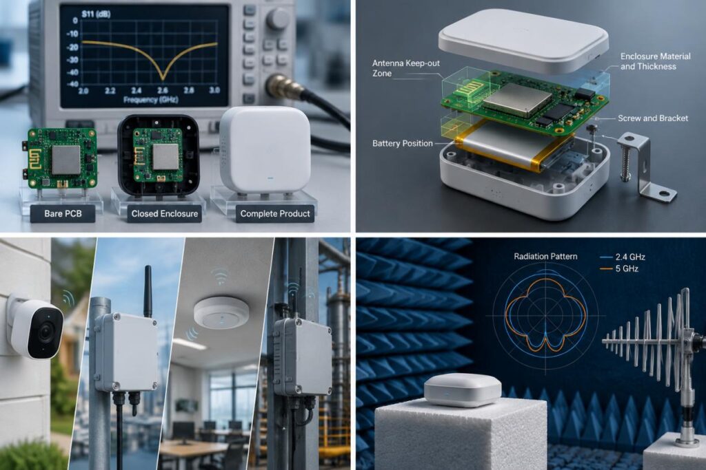
While working through the start of the IoT Electronic Product Development process and debugging, you should conduct controlled comparisons. These should include the bare PCB, the closed enclosure, and the complete product. Maintain the channel, firmware, transmit power, data rate, orientation, and test distance whilst debugging.
| Observed Problem | Likely Mechanism | First Diagnostic Step |
| Performance drops after closing the housing | Detuning, shielding, or changed coupling | Compare impedance and radiated performance |
| Reception worsens when the display operates | Receiver desensitization from internal noise | Compare reception with noise sources enabled and disabled |
| Device fails against a metal wall | Mounting-induced pattern or impedance changes | Test the intended backplate and spacing |
| Potting changes frequency coverage | Dielectric loading and material loss | Compare cured material configurations |
| Production units behave differently | Placement, contact, or material variation | Inspect assembly dimensions and test multiple units |
Separate transmit and receive problems. Increasing transmit power cannot correct a receiver impaired by internal interference.
2. Read Matching Results Alongside Radiation Performance
S11 Does Not Establish Antenna Efficiency
S11 of −10 dB corresponds to approximately 10% reflected power. The accepted power may still be dissipated in conductors or dielectric materials.
At the same reference plane:
Total efficiency = radiation efficiency × (1 − |Γ|²)
For example, 50% radiation efficiency with 10% reflected power produces approximately 45% total efficiency. This is an illustrative calculation, not a product specification.
TI’s reference design documents separate matching, radiation-pattern, and output measurements, including changes caused by plastic encapsulation and ground geometry.
Material and Geometry Changes Interact
IoT Electronic Product Development must account for the following considerations:
• Dielectric Constant: Impacts loading of electromagnetic waves and resonances.
• Loss Tangent: Indicates dielectric dissipation.
• Ground Geometry: Changes the paths and impedance and the radiation of currents.
• Realized Gain, Pattern, and Polarization: Determine the performance of directional links.
• Bandwidth: Meets the required channel specifications when installed.
A matching network is able to help with some degree of impedance matching issues, but cannot help with complete shielding nor the absorption of materials.
3. Compare Antenna Options Within the Available Housing
Evaluate, for IoT Electronic Product Development, the installation of a complete antenna, including the ground, cables, assembly, and validation.
| Technical Choice | Favor the First Option When | Favor the Alternative When | Main Constraint |
| PCB vs. ceramic antenna | Board-edge space supports the reference geometry | A smaller radiating element is needed | Ceramic parts still require ground and clearance |
| Board-mounted vs. FPC antenna | PCB placement provides acceptable radiation | A housing location offers better clearance | FPC placement, adhesive, and feed losses |
| RF window vs. external antenna | An integrated, protected antenna is preferred | Metal obstruction favors external placement | Window integration versus sealing and impact exposure |
| Plastic vs. mixed metal/plastic enclosure | Mechanical and thermal needs permit plastic | Metal is needed for strength or heat spreading | Material loading versus conductive geometry |
| Reference vs. custom antenna design | Reference integration conditions can be preserved | Product geometry requires substantial adaptation | Development cost, validation effort, and ownership |
Catalog gain alone cannot establish the best choice. Compare assembled performance across frequency and installation orientation.
4. Freeze RF Constraints Before Tooling Release
Coordinate the Battery, PCB, and Enclosure
We cover hardware debugging and manufacturability support in our IoT Electronic Product Development scope. The next step is to take the RF requirements and produce controlled drawings and instructions for assembly.
Specify:
• Three-dimensional antenna keep-outs and ground-plane boundaries.
• Battery, display, shielding-can, screw, and harness positions.
• Resin grade, coating, wall thickness, adhesive, and potting coverage.
• FPC position tolerances, cable routing, and connector engagement.
• Concurrent radio modes and worst-case digital activity.
Different antennas require different spacing. Design around the materials surrounding the antenna.
Set Link and Power Budgets
Set a receiver sensitivity value which meets a target packet error rate. Add margin for variation in propagation, orientation, manufacturing and interference. Poor links increase retransmissions and battery usage.
A prototype housing made from different material or without the final coating cannot close production RF validation.
5. Control Installation and Service Changes
IoT Electronic Product Development acceptance should include intended brackets, metal backplates, user proximity, and mounting orientations.
When installing external antennas, consider the length of the installation cable, connector torque, sealing, and strain relief. Account for signal loss in the increased separation of the antennas.
Follow the service guidelines to use only approved antennas and batteries. Replacement of any housing material, coatings, or any routing of cables requires an impact assessment on the RF system. Wireless device operation in the presence of water requires further documentation.
6. Validate the Final Product Beyond Impedance Matching
| Verification | Required Evidence |
| VNA measurement | Calibrated reference plane, controlled cable routing, full-band results |
| OTA measurement | Efficiency, radiation patterns, and applicable total radiated power/total isotropic sensitivity |
| Application test | Packet errors, reconnect behavior, and operating current |
| Production/environmental evaluation | Sample distribution and results after specified stresses |
Identify compliance requirements early. Check approved antenna types, gain limits, RF exposure, and simultaneous-transmission conditions before relying on module approvals.
Confirm applicable RED requirements for Europe and verify ingress claims under IEC 60529.
7. Purchase Defined Engineering Deliverables
An IoT Electronic Product Development quotation should identify:
• Who will cover the costs of tuning, mechanical adjustments, and re-testing.
• Engineering, tooling, compliance-support, and production-test costs.
• Acceptance limits, sample quantities, and test configurations.
• Who will cover the costs of CAD, firmware, matching values, and raw data.
• Approved alternatives, traceability, and change-control requirements.
At LKK Design, we assist clients in development by providing DFM, pilot production and manufacturing coordination. Bring your enclosure concept, target markets, and installation conditions to a comprehensive IoT Electronic Product Development review by LKK Design and we will suggest an integration and verification plan.
FAQs
Q1. What Does LKK Design’s IoT Electronic Product Development Service Include?
LKK Design provides industrial design, hardware and PCB development, embedded firmware, wireless connectivity, cloud platforms, and mobile applications. Its services also cover DFM reviews, certification support, and production coordination, connecting product design with manufacturing requirements.
Q2. Can LKK Design Support Antenna and Enclosure Co-Design?
Yes. LKK Design offers antenna design, RF debugging, industrial design, and mechanical engineering among its services. For antenna and enclosure co-design, the project scope should address PCB geometry, battery placement, housing materials, mounting conditions, and assembled-device validation.
Q3. Can LKK Design Investigate Wireless Performance Loss After Enclosure Assembly?
LKK Design offers RF debugging and hardware debugging services. A useful investigation compares the bare PCB, closed enclosure, and installed device under consistent conditions to distinguish antenna detuning, shielding, feed losses, and receiver interference.
Q4. How Should Buyers Compare Antenna Options With LKK Design?
Provide the operating bands, enclosure dimensions, PCB layout, battery position, and intended mounting arrangement. Compare PCB, ceramic, FPC, and external antennas against ground requirements, clearance, efficiency, assembly tolerances, cable losses, and total integration cost.
Q5. Which Wireless Technologies Does LKK Design Support?
LKK Design offers Wi-Fi, Bluetooth, Zigbee, Z-Wave, Thread, LoRa, NB-IoT, LTE Cat M1, and 4G/5G among its connectivity capabilities. Selection should consider coverage, data volume, power consumption, infrastructure, and target-market requirements.
Contact Us



- 20+ Design Industries Serviced
- 200+ Product Categories
- 1,000+ Industry Leaders Served
- 10,000+ Products Successfully Launched

Founder and Chairman of LKK Design Group
Ready to get started? Connect with us today!
 Talk to Our Team