

 Home /
How to Choose an Electronics Design Partner: A Technical and Procurement Guide


Table of Contents


How to Choose an Electronics Design Partner starts with one question: can the team demonstrate that its design will satisfy the product specification and remain testable, compliant, and manufacturable at the intended volume? A polished prototype or low PCB-design quotation cannot establish that. Buyers need engineering evidence, defined acceptance gates, and ownership of the resulting technical package.
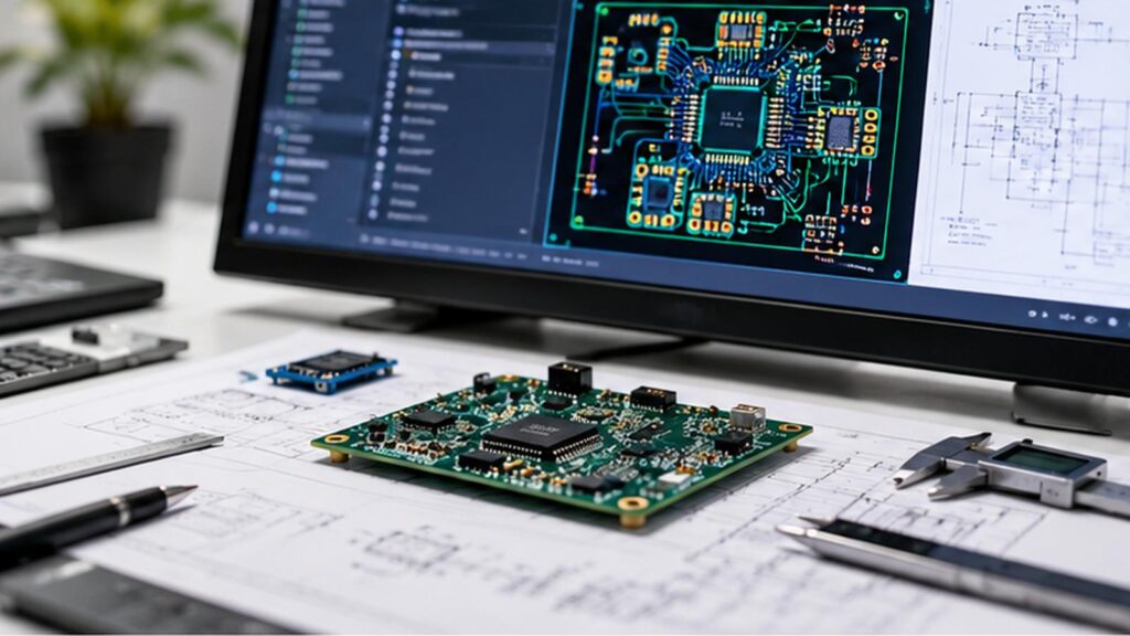
1. Translate Requirements into Quantifiable Engineering Limits
The issuance of a Product Requirements Document (PRD) specifies operating conditions, defines target markets, establishes volumes, and states cost ceilings and pass/fail criteria. You should be asking design candidates to identify design constraints and not just verify design alternatives.
| Requirement | Engineering Trade-off | Evidence to Request |
| Battery life | Average current depends on operating-mode current and duty cycle | Power budget and measured sleep/peak current |
| Compact PCB | Layer count, return paths, thermal dissipation, antenna keep-out | Preliminary stack-up and placement review |
| Target unit cost | MCU selection, component availability, assembly complexity | Costed BOM and approved alternate parts |
For a Bluetooth sensor, reducing enclosure size can detune the antenna; moving a regulator may affect EMI. Competent partners surface these dependencies during architecture review.
2. Audit Electronics, Firmware and Cross-Functional Capability
Assess Actual Engineering Work
Review anonymized examples of deployed product designs to identify engineering and analysis errors, weaknesses in firmware architecture, and potential issues revealed by embedded-system block diagrams.
PCB designs for:
• Power tree and Decoupling
• Control high speed nets by defining impedance and ESD protections
Assess firmware for ownership of drivers and BSP, the selection of an RTOS, if and how watchdogs are recovered, the use of low-power states and if secure OTA updates are implemented.
Evaluate firmware and sourcing decisions including:
• Component lifecycle and second sourcing
• Supply Chain and BOM risk management.
• A product consisting of interconnected systems requires integrated hardware, firmware, mechanical and RF design.
LKK Design has integrated capabilities for the design and development of electronic products, including mechanical, electronic and software design and integration. The potential synergies must still be assessed on a case-to-case basis.
The manufacturing engineers will review the PCB revision anyway. Ask when. And you should definitely check if they’ve completed their DFM checklist.
3. Alternative Engagement Models and Total Program Cost
| Model | Suitable When | Main Exposure |
| Integrated design partner | Several disciplines must converge before tooling | Verify depth of assigned specialists |
| Specialist design firm | One difficult subsystem dominates risk | Client owns integration interfaces |
| In-house team | Product roadmaps require sustained internal iteration | Staffing, equipment, and capacity |
• Pre-certified wireless modules: Contracted service reduces risk and expedites development, but increases cost.
• Custom-made PCBs and RF modules: Higher design risk and more RF validation, in exchange for integration flexibility and lower unit cost at volume.
Budget for:
Total Development Cost = NRE + Prototypes + Redesigns + Testing/Certification + Tooling + Pilot Builds + NPI
For flexibility, use milestone contracts and state upfront what changes mean for the next milestone. Each side should define and agree to acceptance criteria.
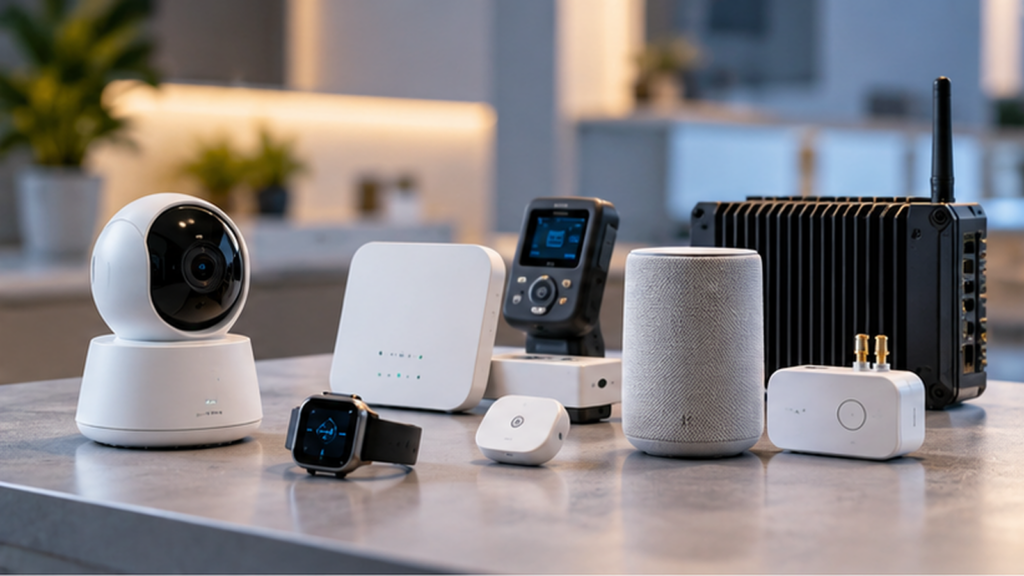
4. Demand Stage-Gate Evidence, Not a Working Prototype
Understanding How to Choose an Electronics Design Partner means separating functional demonstration from production readiness.
At LKK Design, our development framework follows Concept → EVT → DVT → PVT → Mass Production. Each gate should close a different risk:
| Gate | Required Evidence Before Release |
| Concept | Approved PRD, architecture alternatives, risk register |
| EVT | Measured functional/power/RF results; prioritized defect log |
| DVT | Requirements traceability, reliability and EMC pre-compliance tests, design freeze criteria |
| PVT | Production-intent tooling, test coverage, pilot yield, work instructions |
| MP | Controlled BOM, first-pass yield trends, corrective-action and ECO records |
For PVT, ask for build quantity, defect Pareto, rework rates, and repeatability—not an unqualified “high yield” claim.
A prototype that passes a bench test can still fail assembly, environmental testing, or line-level programming.
5. Define Compliance, IP and Lifecycle Requirements
Identify the destination market before PCB design. Depending on product classification, the compliance plan may include:
• FCC Part 15: Requirements for unlicensed US radio frequency devices.
• EU RED/EMC/RoHS: Relevant European radio, electromagnetic compatibility, and hazardous-substance requirements.
• IEC 62368-1: Safety requirements for applicable electronic equipment.
• IPC-2221/IPC-A-610: Printed-board design and electronic assembly acceptability criteria.
These are not interchangeable approvals; a pre-certified radio module does not automatically establish final-product compliance.
Before signing, specify:
• Regulatory ownership: Who prepares technical files, pays for testing, and handles failed-test redesigns?
• IP and handover: Who receives editable schematic/PCB CAD, Gerbers, firmware source, build scripts, BOM/AVL, fixtures, and test reports? An NDA alone does not transfer IP.
• Lifecycle support: Who approves component alternatives, manages end-of-life parts, tracks engineering change orders (ECOs), and investigates field returns?

Final Words
The practical test of How to Choose an Electronics Design Partner is whether requirements can be traced to designs, measurements, and production controls.
We combine various design engineering skills including electronics and embedded design with prototyping, DFM, and production. For detailed understanding of your project requirements, please share your PRD and production estimates. This will help us define the right development scope.
FAQs
Q1: What electronics design services does LKK Design provide?
LKK Design provides hardware architecture, PCB design, embedded firmware development, IoT connectivity, and electronics integration services.
Q2: Can LKK Design handle both PCB design and firmware development?
Yes. LKK Design supports schematic design, PCB layout, embedded drivers, communication protocols, and firmware integration.
Q3: Does LKK Design offer integrated product development?
Yes. LKK Design combines industrial design, mechanical engineering, electronics development, prototyping, and manufacturing support.
Q4: How does LKK Design address Design for Manufacturing (DFM)?
LKK Design integrates DFM analysis, component selection, assembly considerations, and manufacturing feasibility reviews into product development.
Q5: What development stages does LKK Design follow?
LKK Design follows Concept, Engineering Verification Test (EVT), Design Verification Test (DVT), Production Verification Test (PVT), and Mass Production (MP).
Contact Us



- 20+ Design Industries Serviced
- 200+ Product Categories
- 1,000+ Industry Leaders Served
- 10,000+ Products Successfully Launched

Founder and Chairman of LKK Design Group
Ready to get started? Connect with us today!
 Talk to Our Team