

 Home /
 How Electronic Hardware Prototype Development Reduces PCB Design Risks

Table of Contents


A PCB that boots successfully may still be unsuitable for production. Voltage rails can collapse during radio transmission, high-speed interfaces may fail only with long cables, and an antenna can detune after the board enters its enclosure. These are not isolated defects; they are interactions between schematic design, PCB layout, firmware, mechanics, thermal behavior, assembly and component sourcing.
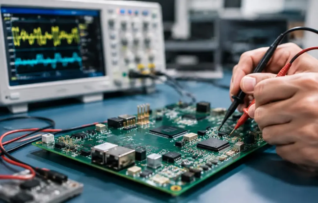
Electronic Hardware Prototype Development reduces these risks by converting design assumptions into measured evidence before certification, tooling and production lock the architecture.
Why Working Samples Still Fail
Early prototypes often appear stable because they are tested at room temperature, powered from laboratory supplies and operated without the final enclosure. Real products introduce more demanding conditions:
• A motor, display or wireless transmitter creates a fast load step.
• Cables extend the EMI coupling path.
• Batteries produce different voltages across their discharge range.
• Plastic or metal housings change airflow and antenna impedance.
• SMT assembly adds solder-joint and component-placement variation.
• Firmware increases processor loading after new features are added.
A functional demonstration therefore proves only that one configuration operated under one set of conditions. Production readiness requires repeatable performance across electrical, mechanical and environmental limits.
Convert PCB Risks into Engineering Measurements
Power integrity should be evaluated from the load rather than from the regulator's nominal rating. A useful starting point is:
[Z_{\text{target}}=\frac{\Delta V_{\text{allowed}}}{\Delta I_{\text{transient}}}]
If a processor rail permits a 40 mV deviation during an 800 mA step, the PDN target is approximately 50 mΩ. Electronic Hardware Prototype Development should then measure startup sequencing, transient droop, ripple, regulator stability and recovery time at the load pins—not only at the power connector.
| Risk domain | Prototype measurement | Design decision |
| Power integrity | Rail droop, ripple, inrush and transient recovery | Regulator, capacitor network, copper and via design |
| Signal integrity | Overshoot, ringing, eye margin and impedance | Stack-up, termination and return path |
| Thermal | Component case temperature and board hot spots | Copper area, thermal vias, spacing and enclosure |
| RF/EMC | Antenna tuning, radiated noise and immunity behavior | Keep-out zone, filters, grounding and shielding |
| Manufacturing | AOI, X-ray, functional test and rework results | Footprints, stencil, test access and process limits |
High-speed risk is governed by signal edge rate, not clock frequency alone. USB, Ethernet, DDR and RF lines may require controlled impedance—commonly 50 Ω single-ended or 90/100 Ω differential, depending on the interface. A correct trace width is insufficient if a signal crosses a plane split or changes layers without a nearby return via.
Select a Prototype That Tests the Intended Product
Different prototype routes answer different questions.
| Approach | Useful evidence | Remaining uncertainty |
| Development board | MCU, sensor and firmware feasibility | Final PDN, layout, EMC, RF and dimensions |
| Four-layer custom PCB | Basic product architecture and integration | Limited routing and reference-plane flexibility |
| Six- or eight-layer PCB | Improved return paths and power distribution | Higher fabrication cost and stack-up control |
| Certified RF module | Faster wireless integration | Host enclosure, antenna and EMC performance |
| Hand-built PCBA | Rapid circuit modification | Automated assembly yield |
| SMT EVT build | Target footprints and assembly process | Long-term reliability and pilot-run consistency |
LKK supports PCBA prototypes from 2 to 12 layers, including fine-pitch devices and BGA/QFN assembly. Its SMT capability covers components from 01005 packages to irregular parts up to 60 mm. These specifications matter because engineers can test the intended processor, memory and power packages instead of using oversized substitutes that hide routing, thermal and assembly risks.
Match the PCB with Firmware, Enclosure and Supply Chain
Before layout release, the team should connect product requirements to worst-case engineering conditions:
• Peak current for radio transmission, motor startup and CPU-intensive firmware;
• Maximum ambient temperature and permitted junction temperature;
• Cable length, connector pinout and external ESD exposure;
• Antenna clearance from batteries, displays, metal parts and user contact;
• Critical-component lifecycle, lead time and second-source availability;
• Target markets and required safety, RF and EMC tests.
Integrated System-Level Prototype Validation
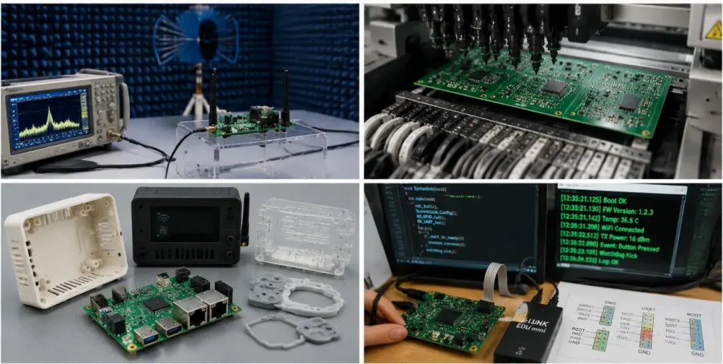
LKK coordinates industrial design, mechanical engineering, electronics and firmware within one product architecture. This enables thermal and EMC simulations to reflect the actual PCB layout, component positions and enclosure.
• Verify connector and PCB alignment.
• Evaluate heatsink contact and thermal paths.
• Confirm antenna clearance in the intended housing.
• Test DVT units under realistic mechanical conditions.
| Process | Technical Capability | Validation Value |
| CNC Machining | ±0.05 mm tolerance; Ra ≤0.8 μm | Accurate housings for fit, thermal and RF testing |
| Vacuum Casting | Approximately 50–200 parts | Supports DVT and market-test batches |
| Material Options | ABS-like, PC-like and transparent materials; Shore A 50–90 elastomers | Simulates production plastics, seals and soft-touch parts |
This integrated approach produces stronger system-level evidence than testing a production PCB inside a generic prototype enclosure.
Design for Assembly, Debugging and Maintenance
A compact layout that cannot be tested is not production-ready. Critical rails, reset lines, clocks and communication buses need accessible test points. SWD/JTAG, UART, boot-control and recovery interfaces should be placed before routing is frozen.
The prototype should also verify:
• Connector insertion force and mounting stress;
• Programming and functional-test access after enclosure assembly;
• Cable strain relief, shield termination and chassis grounding;
• Firmware logs, watchdog recovery and fault codes;
• Rework clearance around high-risk components.
In LKK's Electronic Hardware Prototype Development workflow, DFM review, PCBA assembly, issue tracking and engineering-change control connect prototype findings with manufacturing data. This prevents undocumented jumper wires or manual adjustments from entering production.
Use EVT, DVT and PVT as Evidence Gates
EVT verifies architecture, power rails, boot behavior, critical interfaces, SI, temperature and initial RF performance. DVT uses the intended PCB, BOM and enclosure for reliability and pre-compliance testing. PVT validates SMT settings, programming, inspection coverage, functional fixtures and pilot-run consistency.
Relevant references may include IPC-2221/2222 for PCB design, IPC-2152 for current-carrying capacity, IPC-6012 for rigid-board performance, and IPC-A-610 or J-STD-001 for assembly.
Depending on the product, FCC Part 15, RED, CISPR requirements, IEC 61000-4 immunity tests, RoHS and product-specific safety standards may also apply. Applicability and current editions must be confirmed for each market.
Procure Evidence, Not Just Prototype Boards
An Electronic Hardware Prototype Development quotation should specify ownership of schematic and PCB source files, Gerber data, BOM, approved vendor list, firmware, test reports, issue logs and ECNs. It should also define responsibility for component substitutions, EMC redesign and retesting.
LKK combines PCB engineering, firmware, enclosure prototyping, BOM optimization, DFM and pilot-production support. Teams developing products with high-speed interfaces, wireless connectivity or tight thermal constraints can engage LKK early to build a risk-based validation plan before the first production-intent PCB is released.
FAQs
Q1. What does LKK's Electronic Hardware Prototype Development service include?
LKK provides hardware architecture, schematic design, PCB layout, BOM creation, PCBA fabrication, embedded firmware, functionality testing, DFM evaluation and production preparation.
Q2. How many PCB layer counts does LKK support?
LKK performs PCBA prototyping for boards ranging from 2-12 layer PCBs. The appropriate layer count is dependent on routing density, power distribution, controlled impedance and EMC.
Q3. Does LKK perform assembly of fine-pitch and complex electronic components?
Yes it does. LKK works with fine-pitch devices, BGA (ball grid array) and QFN (quad flat no leads) packages. In SMT (surface mount technology) LKK works with components as small as 01005 to large irregular size components up to 60 mm.
Q4. What does LKK do to mitigate PCB power integrity?
During prototype testing, LKK evaluates power integrity by analyzing the power architecture, selection of regulators, power sequencing, decoupling, load transients, voltage ripple and power distribution.
Q5. Does LKK do high-speed PCB design?
Yes. High-speed PCB design by LKK covers all aspects of controlled impedance, stack-up, differential routing and reference plane continuity, and signal integrity.
Contact Us



- 20+ Design Industries Serviced
- 200+ Product Categories
- 1,000+ Industry Leaders Served
- 10,000+ Products Successfully Launched

Founder and Chairman of LKK Design Group
Ready to get started? Connect with us today!
 Talk to Our Team