

 Home /
 PCB and Enclosure Co-Design for Electronic Products | Beginner's Guide


PCB and Enclosure Co-Design for Electronic Products: Guide
- A product may fail as a physical product even though it has a great circuit. The PCB can be tested on the bench and be fine, but the connectors do not fit the enclosure. A battery can be ill-fitting. The heat can accumulate in the housing. A button can be too close to a wall. Even a couple of millimeters of unforeseen interference may require a costly redesign.
- This is why PCB and Enclosure Co-Design for Electronic Products must occur as a single, related process and not two design activities. The electrical system is defined by PCB engineers and the physical product is designed by mechanical teams. By collaborating early on, the outcome can be smaller, more dependable, easier to put together, and more production-friendly.
Why PCB and Enclosure Design Must Begin Simultaneously
Conventional workflows tend to consider PCB design and enclosure design as distinct processes. The electronic team develops the board and the mechanical team attempts to package it. That strategy might be effective with simple products, but the new devices are getting smaller and smaller. IoT products, wearable devices, smart sensors, and industrial controllers tend to have minimal unused space. PCB enclosure co-design is a more effective solution, where electrical and mechanical decisions are made jointly.
The teams are in constant comparison:
• Height and internal clearance of components.
• Mechanical supports and PCB mounting holes.
• External ports and connector positions.
• Battery position and capacity.
• Components and airflow that produce heat.
• Access to cable routing and assembly.
• Enclosure wall thickness
• Mounting features and fasteners.
• User-accessible controls
This enhances integration of PCB enclosures and minimizes surprises in the later stages of development.
Start With the Product Architecture
The product must have a clear physical and electrical architecture before detailed CAD or routing is done. The PCB architecture specifies key electrical functions, interfaces, components, power paths, communication systems, and board requirements. Meanwhile, the mechanical concept determines the shape of the product, mounting plan, user interfaces, and internal volume.
- As an example, a product with electronics components, such as a processor, battery, wireless module, display, sensors, and USB connector, cannot be designed around the PCB. All these elements should be enclosed and spaced appropriately and accessibly.
- This is where the design of electronics products is a cross-functional task that includes industrial design, mechanical engineering, electronics engineering, and product engineering.
PCB Layout Has an Impact on the Physical Enclosure
PCB is not a mere flat board with components. The layout is capable of directly influencing the shape and size of the final product. When laying out a PCB, engineers take into account the placement of components, routing, power distribution, signal integrity, thermal behavior, and manufacturing considerations. At the same time, the mechanical team needs information about:
• Board width and length.
• Maximum component height
• Connector locations
• PCB mounting holes
• Keep-out regions
• Heat-generating components
• Antenna locations
• Cable exits
• Test points
• Service access
As an example, a tall capacitor or connector placed close to an enclosure wall could cause a mechanical clearance issue. The physical problem can be resolved by relocating the component, but this can impact routing or signal performance. That is why the placement of PCB components and enclosure geometry should be discussed simultaneously.
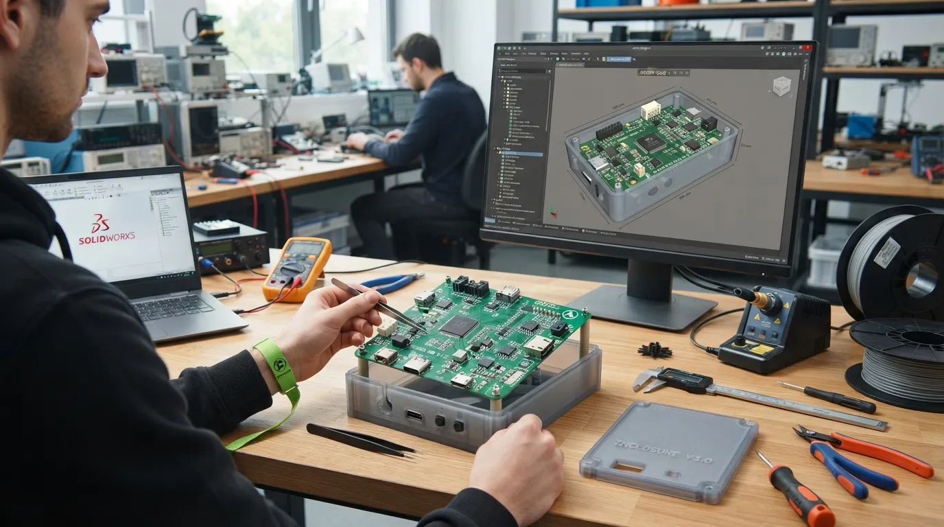
PCB Clearance and Mechanical Clearance
One of those little things that can cause very big problems is clearance. PCB clearance is defined as the space that is needed around components, conductors, mounting features, and other electrical elements. Mechanical clearance deals with the physical area that is needed between the components and the structures around them.
Both should be taken into consideration when integrating PCBs mechanically. As an illustration, a connector can need sufficient space to insert and remove the plug. A screw head might require clearance over the PCB. A heat sink can be larger than the anticipated height of the component.
An effective clearance review must look at:
• Component-to-wall spacing
• Component-to-component spacing
• PCB-to-enclosure spacing
• Connector access
• Fastener clearance
• Cable bending radius
• Assembly tool access
• Service access
These are particularly crucial when handling small electronics.
Enclosure Beginning of Thermal Management
Another reason why electrical and mechanical teams should work together is heat. A processor, power converter, motor driver, LED, radio module, or charging circuit may produce a lot of heat. If the enclosure captures such heat, internal temperatures may increase and impact reliability. As part of its development strategy, LKK has electronics engineering capabilities, such as thermal simulation and thermal profiling. It also includes thermal analysis and PCB and hardware development in its electronics service.
A co-design workflow can evaluate:
• Heat-producing components
• Heat paths
• Heat sinks
• Thermal interface materials
• Airflow
• Vent locations
• Enclosure materials
• Internal temperature
• Ambient operating conditions
Passive cooling can be sufficient with certain products. Others might need vents, conductive materials, heat spreaders, or active cooling. The most important thing is that thermal performance is not a PCB and Enclosure Co-Design for Electronic Products issue. It is a system problem.
Placing of Components Ought to Be Based on the End Product
Placement of electronic components is usually optimized to achieve electrical performance, but mechanical considerations must be considered simultaneously. Take an example of a wireless product. The antenna might require a special position to be in operation. The design might be influenced by a metal bracket that is too close to it. A battery can be required to fit a specific area. The position of the board can be determined by a display. This is the reason why placement of components should take into account:
• Electrical performance
• Thermal behavior
• Mechanical clearance
• Assembly
• Serviceability
• Cable routing
• Enclosure geometry
• User interaction
Even a slight modification of the board can reduce the whole enclosure to a simple one.
Conclusion
A PCB is the electronic core of a product, and the enclosure secures it, locates it, and forms the way in which people use it. Their treatment as distinct designs can bring about unwarranted compromises. Need a physical design that is production-ready and precision-engineered? Discuss with LKK to have the PCB, enclosure, and entire hardware system assembled initially.
Contact Us



- 20+ Design Industries Serviced
- 200+ Product Categories
- 1,000+ Industry Leaders Served
- 10,000+ Products Successfully Launched

Founder and Chairman of LKK Design Group
Ready to get started? Connect with us today!
 Talk to Our Team