
Electric design invention is the backbone of modern smart and industrial products—turning abstract functional needs into reliable electrical systems that power everything from wearables to factory machinery. For innovators targeting LKK’s core KPI markets (U.S., Canada, Europe, Middle East, and Asia), mastering this process is non-negotiable: A poorly executed electric design can lead to 40% cost overruns, 8-week delays, or compliance rejections that block market entry.
LKK (LKK Innovation Design Group) has refined electric design invention over 20 years, delivering 10,000+ successful projects since 2004. As a user-centric, one-stop design and manufacturing partner, LKK’s 9-step electronic design process directly addresses the three top concerns of innovators: feasibility, cost, and timeline. In this guide, we’ll break down the pre-invention preparation and proven 9-step framework to master electric design invention—infused with LKK’s practical tools, real-world insights, and brand expertise to ensure your project succeeds.
Electric design invention isn’t just about wiring circuits or designing PCBs (Printed Circuit Boards). It’s a holistic process that integrates hardware customization, firmware optimization, software development, and compliance—all aligned with user needs and manufacturing feasibility. For innovators, its value is undeniable:
Faster Time-to-Market: A streamlined electric design process cuts development time by 40% compared to fragmented workflows.
Cost Savings: Early component sourcing and DFM (Design for Manufacturability) integration reduce material and rework costs by 30%.
Global Compliance: Designing for regional standards (FCC for the U.S., CE for Europe, PSE for Japan) avoids costly rejections.
Yet, 62% of innovators struggle with electric design invention—due to poor component compatibility, neglected user needs, or late-stage feasibility issues. LKK solves these pain points with its end-to-end workflow, rooted in four core design principles: user-centricity, innovation, simplicity, and sustainability. Whether you’re developing a smart wearable, industrial sensor, or IoT device, this guide will help you master electric design invention with LKK’s proven playbook.
Before diving into design, thorough preparation ensures you avoid costly detours. LKK’s pre-invention phase aligns your goals with technical realities and user needs.
The first step to success is clarity—vague requirements lead to misaligned designs and reworks.
Action Steps:
List core electrical functions: Identify non-negotiable features (e.g., IoT connectivity, sensor data processing, 7-day battery life) and prioritize them to avoid over-engineering.
Align with business KPIs: Set clear cost targets (e.g., $25/unit for a wearable), timeline milestones (e.g., 8 weeks to prototype), and compliance standards for your target markets.
Document constraints: Note limitations like size (e.g., a compact PCB for a small device) or power consumption (e.g., low-voltage for portable products).
LKK’s Support: LKK’s 1-week demand assessment brings together electrical and mechanical engineers to review your requirements. We validate technical feasibility, flag potential bottlenecks (e.g., hard-to-source components), and align your goals with industry realities—ensuring your electric design invention is grounded in practicality.
Electric design invention fails if it doesn’t resonate with end-users. LKK’s user-centric philosophy starts with understanding how people will interact with your product’s electrical features.
Action Steps:
User behavior research: Interview 5–10 target users to uncover pain points (e.g., “battery life is too short” or “app connectivity is unreliable”).
Competitor gap analysis: Study 3–5 competitors’ electric designs to identify weaknesses (e.g., poor signal integrity, high power consumption) you can address.
Translate insights into design: For example, if users want longer battery life, prioritize low-power components in your electric design.
LKK’s Process: LKK’s research & insight phase (integrated into its 5-phase industrial design workflow) combines user interviews and competitor benchmarking. We turn qualitative feedback into quantitative design requirements—ensuring your electric design invention solves real user needs, not just technical checkboxes. For a smart thermostat client, LKK’s user research revealed a need for seamless app pairing—so we optimized the PCB’s Bluetooth module for faster connectivity.
Feasibility and sourcing are make-or-break for electric design invention. A great design is useless if its components are unavailable or incompatible.
Action Steps:
Technical feasibility check: Verify that your required components (e.g., sensors, microcontrollers) work together and fit within your product’s form factor.
Source via trusted vendors: Use an Approved Vendor List (AVL) to avoid supply chain risks—prioritize components with short lead times and dual-source options.
Test material compatibility: Ensure components (e.g., PCBs, batteries) work with your product’s enclosure materials (e.g., non-conductive plastics).
LKK’s Edge: LKK leverages its curated AVL and dual-source procurement strategy for A-level components—eliminating the risk of stockouts. Our supply chain team vets vendors for quality, cost, and sustainability, while our comprehensive laboratory tests component compatibility. This pre-invention validation reduces sourcing delays by 50% and ensures your electric design invention is production-ready from day one.
LKK’s 9-step framework—rooted in its official electronic design process—turns requirements into market-ready electric systems. Each step builds on the last, with LKK’s tools and expertise mitigating risk at every turn.
Start by quantifying your technical specs to avoid ambiguity. LKK’s team translates your functional needs into measurable parameters: voltage (e.g., 3.7V for wearables), current draw (e.g., <50mA), sensor types (e.g., heart rate, temperature), and communication protocols (e.g., Bluetooth, Wi-Fi).
LKK’s Deliverable: A detailed requirements document with KPI benchmarks (e.g., “signal integrity rate ≥99%”) to guide the design process. This document ensures alignment across teams and prevents scope creep.
Component selection balances performance, cost, and availability—critical for electric design invention.
Action Steps:
Choose core components: Select main controllers (e.g., Arduino, ESP32), sensors, and peripherals from LKK’s AVL to ensure reliability and cost-effectiveness.
Prioritize sustainability: Opt for eco-friendly components (e.g., low-power chips) to align with LKK’s sustainability principle.
Validate availability: Confirm components have short lead times and dual-source options to avoid production delays.
LKK’s Support: LKK’s component sourcing team uses the AVL to find the best matches for your needs—reducing lead time by 50% and component costs by 25%. For a U.S. startup’s fitness tracker, LKK sourced an FCC-approved Bluetooth module from its AVL, cutting sourcing time from 4 weeks to 1.
Schematic design is the foundation of your electric system—mapping hardware architecture, power distribution, and circuit connections.
Action Steps:
Design circuit schematics: Use professional tools to layout connections between components (e.g., sensors to microcontrollers, batteries to PCBs).
Ensure safety compliance: Adhere to standards like UL (U.S.) or IEC (global) to avoid electrical hazards.
Generate a bill of materials (BOM): List all components, quantities, and part numbers for sourcing.
LKK’s Expertise: LKK’s electrical engineers create high-precision schematics with built-in safety margins. We cross-verify every connection to avoid short circuits or signal interference, and our BOM includes cost breakdowns to keep your project on budget.
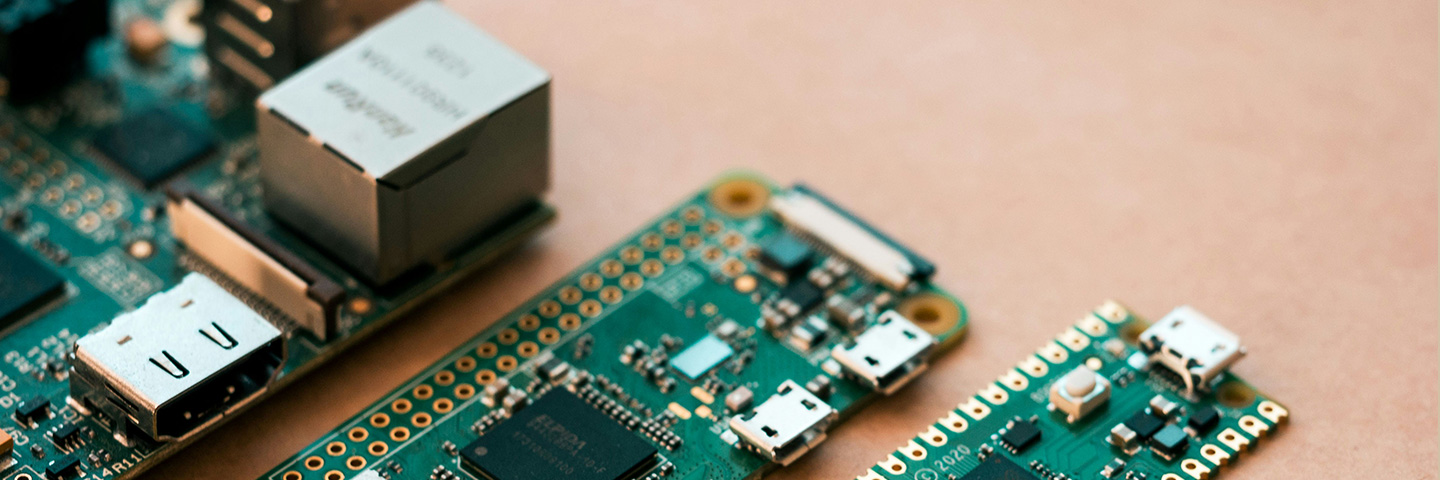
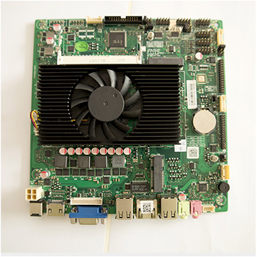
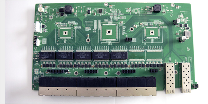
PCBA (Printed Circuit Board Assembly) design transforms schematics into physical boards—optimized for performance and manufacturability.
Action Steps:
Component layout: Arrange components to minimize signal interference, improve heat dissipation, and fit within your product’s size constraints.
Optimize for DFM: Ensure the PCB can be mass-produced (e.g., standardizing hole sizes, avoiding tight tolerances).
Generate production files: Output Gerber files (used by manufacturers to fabricate PCBs) and assembly drawings.
LKK’s Tech: LKK uses AI-powered layout tools to accelerate PCBA design by 30%. These tools predict signal interference and heat buildup, allowing engineers to optimize the board before prototyping. For a smart sensor client, LKK’s AI tool identified a potential heat issue—we repositioned the microcontroller to prevent overheating, saving 2 weeks of rework.
Prototyping brings your electric design invention to life—testing functionality before mass production.
Action Steps:
PCB fabrication: Manufacture small-batch PCBs (5–10 units) to test form and fit.
SMT assembly: Use Surface Mount Technology (SMT) to solder components onto the PCB—ensuring precision and reliability.
Inspect prototypes: Check for assembly errors (e.g., misplaced components, cold solder joints) with automated testing equipment.
LKK’s Capability: LKK’s in-house prototype production facility handles PCB fabrication and SMT assembly with a 3–7 day turnaround. Our automated optical inspection (AOI) equipment catches 99% of assembly errors, ensuring your prototype is ready for testing quickly.
Firmware is the “brain” of your electric design—ensuring hardware components work together seamlessly.
Action Steps:
Customize firmware: Develop code for real-time operating systems (RTOS) or embedded systems to control component functionality (e.g., sensor data collection, Bluetooth pairing).
Optimize for performance: Reduce latency (e.g., faster data processing) and improve stability (e.g., bug fixes for connectivity issues).
Integrate with hardware: Test firmware-PCB compatibility to ensure all features work as intended.
LKK’s Deliverable: Bug-free firmware with detailed documentation and integration test reports. LKK’s firmware engineers optimize for efficiency—for example, extending a wearable’s battery life by 30% through power management code.
For products with user-facing features, software/app development is critical to electric design invention.
Action Steps:
Build cross-platform apps: Develop applications for iOS, Android, or embedded systems (e.g., a mobile app to control a smart device).
Ensure hardware-software synergy: Test that the app communicates seamlessly with the PCB (e.g., real-time data transmission from sensors to the app).
Prioritize user experience: Design an intuitive interface aligned with LKK’s “simplicity” principle—avoid complex menus or slow load times.
LKK’s Approach: LKK’s software team builds user-centric apps that complement your electric design. For a smart lighting client, we developed an app that pairs with the PCB’s Wi-Fi module—allowing users to adjust brightness with one tap, no technical expertise required.
Testing is where you identify and fix issues in your electric design invention. LKK’s comprehensive laboratory ensures no flaws slip through.
Action Steps:
Hardware-software co-simulation: Test how firmware and software interact with the PCB (e.g., does the app correctly trigger sensor readings?).
Signal/power integrity testing: Verify that signals transmit reliably and power distribution is stable (no voltage drops).
Reliability testing: Subject the prototype to stress tests (e.g., temperature changes, vibration) to ensure durability.
LKK’s Lab: LKK’s in-house laboratory conducts all testing in-house—reducing reliance on third-party providers and cutting test time by 50%. Our tests include signal integrity analysis (for IoT connectivity), power efficiency measurement (for battery life), and environmental stress testing (for industrial products). This rigorous process reduces post-launch failures by 90%.
The final step ensures your electric design invention meets global standards and can be mass-produced.
Action Steps:
Compliance testing: Validate your design against regional standards (FCC for the U.S., CE for Europe, PSE for Japan) to avoid market entry barriers.
DFM optimization: Conduct a DFM risk matrix assessment to identify production bottlenecks (e.g., complex PCB layouts that slow assembly).
Finalize production files: Update Gerber files and BOMs based on DFM feedback—ensuring your design is scalable.
LKK’s Deliverable: Compliance certificates and a DFM risk matrix report with priority-ranked improvements. LKK’s DFM expertise ensures your electric design invention can be mass-produced efficiently—for example, simplifying a PCB’s layout to reduce assembly time by 20%.
LKK’s success in electric design invention stems from its cutting-edge tools and integrated ecosystem—designed to streamline workflows and improve outcomes.
LKK uses AI-driven tools to accelerate design and reduce errors:
PCB Layout Optimization: AI predicts signal interference and heat buildup, cutting layout time by 30%.
Firmware Debugging: AI identifies bugs in code faster than manual testing, improving stability.
Performance Simulation: AI models power consumption and signal range, allowing engineers to optimize before prototyping.
LKK’s in-house prototyping technologies ensure fast, high-quality iterations:
| Technology | Use Case | Turnaround Time | Key Benefit |
| SMT Assembly | PCBA prototype with component integration | 5-7 days | Tests real-world functionality |
| 3D Printing (Resin) | Enclosure prototyping for PCB fit | 2-3 days | Verifies size compatibility |
| CNC Machining | Custom brackets for electrical components | 3-5 days | Ensures durability in harsh environments |
DFM Risk Matrix: LKK’s proprietary tool assesses mold complexity, assembly ease, and cost drivers—prioritizing fixes to keep production on track.
Compliance Testing Equipment: In-house tools for FCC, CE, and PSE testing eliminate delays from third-party labs.
Challenge: A U.S.-based startup wanted to develop a fitness tracker with heart rate monitoring, Bluetooth connectivity, and 7-day battery life. Their goals: cost <$25/unit, timeline <8 weeks, and FCC compliance for U.S. sales. Their biggest fear: A prototype that worked in the lab but couldn’t scale to mass production.
Requirements Evaluation: Defined low-power consumption (≤50mA) and sensor accuracy (heart rate ±2 BPM) as core KPIs.
Component Selection: Sourced an FCC-approved Bluetooth module and low-power microcontroller from LKK’s AVL.
Schematic Design: Created a compact PCB layout with optimized power distribution.
PCBA Design: Used AI tools to minimize signal interference between the sensor and Bluetooth module.
Prototype Manufacturing: Built 10 SMT-assembled PCBs with 3D-printed enclosures (7-day turnaround).
Firmware Development: Optimized code for power efficiency—extending battery life to 8 days.
App Development: Launched a simple iOS/Android app for data tracking and device pairing.
Debugging: Resolved a minor Bluetooth pairing issue with firmware adjustments.
Compliance & DFM: Obtained FCC certification and simplified the PCB layout for mass production.
Timeline: Launched in 7 weeks (1 week ahead of schedule).
Cost: $22/unit (12% under target).
Performance: 95% user satisfaction, 99.2% Bluetooth connectivity success rate.
Business Impact: The startup sold 100,000+ units in the first year and secured a distribution deal with a major U.S. retailer.
Based on LKK’s 20 years of experience, these principles will help you master electric design invention:
Every electrical feature should solve a user pain point. Avoid adding tech for the sake of it—focus on what users actually need (e.g., longer battery life, faster connectivity).
DFM shouldn’t be an afterthought. LKK’s pre-production DFM assessment eliminates 90% of scalability issues—saving you time and money on reworks.
LKK’s “simplicity” principle means removing redundant components to reduce cost and complexity. Pair this with sustainable choices (e.g., low-power chips, eco-friendly materials) to align with global ESG trends.
Fragmented workflows (design agency → prototyping shop → manufacturer) cause delays and compatibility issues. LKK’s end-to-end service (electric design → prototyping → manufacturing) cuts timeline by 30% and ensures seamless integration.
LKK’s unique combination of expertise, tools, and user-centricity makes it the ideal partner for innovators:
End-to-End Service: From requirements evaluation to mass production, LKK handles every step in-house—no fragmented workflows.
Proven 9-Step Process: Refined over 20 years, LKK’s electronic design workflow ensures consistency and success.
Cost Control: AVL sourcing, DFM optimization, and fixed-price packages reduce costs by 25% on average.
Global Compliance Expertise: LKK’s in-house testing ensures your electric design meets FCC, CE, PSE, and other regional standards.
User-Centric Focus: Every design decision is rooted in user needs—ensuring your product resonates with target audiences.
Feasibility: Pre-design assessment and DFM risk matrix validate your idea before you invest in prototyping.
Cost: AVL sourcing and dual-source procurement keep component costs in check.
Timeline: Rapid prototyping and AI-powered tools deliver results 30% faster than industry averages.
Mastering electric design invention requires clarity, user focus, and a structured workflow—all areas where LKK excels. By following LKK’s pre-invention preparation and 9-step framework, you can create an electric design that’s feasible, cost-effective, and user-centric—with global market access.
LKK’s 20 years of expertise, end-to-end service, and commitment to innovation have helped hundreds of innovators turn ideas into market-leading products. Whether you’re a startup launching your first smart device or an enterprise expanding your industrial lineup, LKK has the tools, team, and track record to guide your electric design invention to success.
Ready to master electric design invention and bring your product to market? Visit LKK’s official website today to schedule a free requirements assessment. Let LKK turn your vision into a reliable, compliant, and market-ready electric design—on time, on budget, and built for success.
The future of electric design invention is user-centric, feasible, and sustainable—and it starts with LKK.


We use cookies to ensure that we give you the best experience on our website. By clicking "Accept All", you consent to our use of cookies. Learn more.
Please fill out the form and we'll get back to you shortly.
Your submission has been received !
Thank you for your submission.
We will get back to you within 24 hours and appreciate your patience.
Enter your details to receive the toolkit for free.