
Today's most exciting products share a common characteristic: they are "smart." They sense, process, connect, and respond to their environment. From wearable health monitors to industrial IoT sensors and smart home devices, electronics are the nervous system of modern innovation. But how does an electronic concept evolve from a theoretical circuit diagram into a physical, working board that powers a revolutionary product? This transformation is the domain of electric design prototyping—the systematic journey from abstract schematic to tangible, functional Printed Circuit Board Assembly (PCBA). It is the critical bridge between an electronic idea and an intelligent, market-ready product.
Before diving into the process, it is essential to understand the destination. The terminology can be confusing for those new to electronics development.
Schematic: The logical blueprint of the circuit. It shows the components and how they are electrically connected, but it does not represent their physical arrangement.
PCB (Printed Circuit Board): The physical board itself—a flat substrate (typically fiberglass) with copper traces that physically realize the connections defined in the schematic.
PCBA (Printed Circuit Board Assembly): The PCB with all electronic components (resistors, capacitors, ICs, connectors) soldered onto it. This is a functional electronic module ready to be programmed and integrated into a product.
The end goal of electric design prototyping is a validated PCBA that executes its intended firmware, interfaces correctly with sensors and actuators, manages power efficiently, and meets all performance and reliability specifications. Achieving this requires a structured, multi-disciplinary process that integrates hardware engineering, firmware development, and rigorous testing.
This holistic approach is precisely how leading design firms operate. LKK Design, for instance, defines its electronic design services as providing "end-to-end development services" spanning hardware customization, firmware development, and software application creation. This comprehensive perspective ensures that every aspect of the electronic product is developed in harmony.
Professional electric design prototyping follows a disciplined, phase-gated workflow. Below is a detailed walkthrough of the eight essential steps, mapped to industry best practices.
Every successful prototype begins with clear specifications. This phase answers fundamental questions:
What is the primary function of the device?
What are the power requirements (battery life, voltage, current)?
What processing power is needed?
What sensors, communication interfaces (Bluetooth, Wi-Fi, cellular), and user I/O are required?
What are the size constraints?
With requirements defined, the critical work of component selection begins. Engineers evaluate microcontrollers, sensors, power management ICs, and connectors based on performance, cost, availability, and long-term supply chain stability. Choosing the right components at this stage prevents catastrophic redesigns later.
In Practice: This aligns directly with the first two steps of a professional electronic design workflow: "Electronic Requirements" (effort assessment and specification development) and "Component Selection" (identifying the main controller solution and sourcing critical parts).
With components selected, the engineer creates the schematic—the logical map of the circuit. Using specialized software (such as Altium Designer, Eagle, or KiCad), each component is placed symbolically, and connections are drawn between pins. This phase includes:
Defining the hardware architecture.
Designing the power distribution network (voltage rails, regulators, decoupling capacitors).
Connecting communication buses (I2C, SPI, UART) between components.
Generating the initial Bill of Materials (BOM)—a complete list of every component required.
The schematic is the foundational document from which everything else flows. Errors here propagate through the entire project.
In Practice: Professional firms execute this as a dedicated "Schematic Design" phase, encompassing hardware architecture planning, power distribution design, circuit design, and BOM generation.
The schematic is now translated into a physical board layout. This is both an art and a science, requiring careful consideration of:
Component Placement: Positioning components to minimize trace lengths, optimize thermal performance, and fit within mechanical enclosure constraints.
Trace Routing: Drawing the copper connections between components. High-speed signals (like USB or RF) require controlled impedance and careful routing to avoid interference.
Power and Ground Planes: Dedicated layers or large copper areas to distribute power cleanly and minimize noise.
Thermal Management: Adding thermal vias and copper pours to dissipate heat from power components.
Design Rule Check (DRC): Verifying that the layout meets manufacturing constraints (minimum trace widths, clearances, hole sizes).
The final output of this phase is a set of Gerber files—the manufacturing standard for fabricating PCBs.
In Practice: This corresponds to the "PCBA Design" step, where experts focus on component placement optimization and Gerber file output.
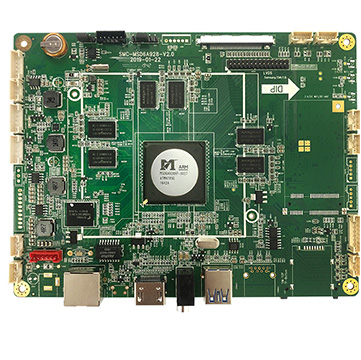
The design now leaves the digital realm. The Gerber files are sent to a PCB fabrication house, which produces the bare circuit boards. Simultaneously, components are sourced based on the BOM. The boards and components then go to an assembly house, where Surface Mount Technology (SMT) machines place and solder the components onto the board with incredible precision.
The result is the first physical PCBA prototype—a tangible representation of your electronic idea.
In Practice: This is the "Prototype Manufacturing" stage, covering PCB fabrication and SMT assembly, delivering the first hardware for testing.
A board full of components is inert without code. Firmware is the low-level software that runs on the microcontroller, directly controlling the hardware. This phase involves:
Setting up the development environment and Real-Time Operating System (RTOS) if needed.
Writing drivers to interface with peripherals (sensors, displays, communication modules).
Implementing the core application logic that defines the product's behavior.
Debugging using tools like JTAG programmers and logic analyzers.
Firmware development often runs in parallel with hardware prototyping, with initial testing done on development boards before the custom PCBA arrives.
In Practice: This is the dedicated "Firmware Development" phase, including RTOS/firmware customization and peripheral driver integration.
For products that interact with users via smartphones or computers, application software development is required. This includes:
Mobile Apps: iOS and Android applications that communicate with the device via Bluetooth or Wi-Fi.
Desktop Software: Applications for configuration, data analysis, or control.
Embedded UIs: User interfaces on built-in screens.
These applications implement the user-facing logic and provide the interface through which people experience the product's intelligence.
In Practice: This is LKK's "Application Development" stage, delivering scenario-based logic implementation and cross-platform app development.
With the first PCBA in hand and firmware ready, the intense work of validation and debugging begins. This phase includes:
Hardware-Software Co-Simulation: Verifying that the code correctly controls the hardware.
Signal Integrity Debugging: Using oscilloscopes to check that communication signals are clean and meet timing specifications.
Power Analysis: Measuring current consumption to ensure battery life targets are achievable.
Thermal Imaging: Identifying components that overheat under load.
Issues discovered here lead to design refinements, documented through Engineering Change Notices (ECNs).
In Practice: This critical phase is LKK's "Functional Debugging" stage, encompassing hardware-software co-simulation and signal integrity debugging.
The final step before declaring the prototype ready for production is rigorous, formal testing against all requirements:
Power Integrity Analysis: Verifying stable, noise-free power delivery to all components.
Signal Integrity Verification: Ensuring all high-speed communication links are reliable.
Reliability Testing: Subjecting the PCBA to thermal cycles, vibration, and extended operation to identify early-life failures.
Safety and Compliance Testing: Validating against regulatory standards (FCC, CE, UL) required for market entry.
Only after passing these tests is the prototype considered validated and ready for the transition to mass production.
In Practice: This final validation aligns with LKK's "PCBA Testing" phase, which comprehensively verifies power integrity, signal integrity, reliability, and safety compliance.
A common misconception is that the first prototype will work perfectly. In reality, "first spin success" is rare, especially for complex designs. Professional engineers embrace this reality, planning for multiple design iterations. Each prototype cycle—build, test, analyze, and refine—uncovers issues and yields a more robust design.
This iterative loop is formalized through Engineering Change Notices (ECNs) , which document every modification, its rationale, and its approval. This creates a clear audit trail and ensures that lessons learned are captured. Professional processes, like LKK's, explicitly incorporate testing reports and engineering change documentation, building iteration into the workflow as a feature, not a bug.
Awareness of frequent failure points can save significant time and cost:
Inadequate Power Distribution: Insufficient decoupling or poorly designed power traces can cause unpredictable behavior and system resets.
Poor Component Selection: Choosing parts with long lead times, pending obsolescence, or inadequate specifications leads to redesigns.
Signal Integrity Problems: In high-speed designs, improper trace routing can cause data corruption and communication failures.
Hardware-Software Integration Mismatches: Disconnects between what the hardware can do and what the software expects are common when teams work in silos.
Skipping Thermal and Reliability Testing: A board that works on the bench may fail catastrophically in a hot enclosure or after thousands of power cycles.
The complexity of modern electronics demands that hardware, firmware, and software evolve together. When these disciplines are developed by disconnected teams, integration becomes a nightmare of finger-pointing and costly rework. The ideal scenario is an integrated approach where all three domains are developed collaboratively from day one.
This is the core value proposition of full-service design firms. LKK Design's end-to-end electronic design services—spanning hardware customization, firmware development, and software application creation—are explicitly structured to eliminate integration risk. Their comprehensive workflow ensures that every piece of the electronic puzzle works together seamlessly from the very first prototype.
A validated prototype is a milestone, not the finish line. The journey to market requires a successful transition to volume manufacturing. This involves:
Design for Manufacturability (DFM) for Electronics: Optimizing the design for high-volume assembly, including panelization, test point access, and component selection for automated placement.
Test Fixture Development: Creating custom fixtures for programming and testing boards on the production line.
Quality Control Planning: Defining inspection criteria and sampling plans.
Scaling with Contract Manufacturing Partners: Engaging with partners who can handle volume production while maintaining quality.
Leading design firms bridge this gap seamlessly. LKK's electronic prototyping capabilities connect directly to their broader manufacturing engineering and contract manufacturing services, ensuring that the transition from prototype to mass production is smooth, predictable, and de-risked.
Electric design prototyping is a structured, multi-disciplinary journey that demands deep expertise in hardware engineering, firmware development, and rigorous testing. It transforms abstract circuit diagrams into the physical intelligence that powers modern products. Success lies not in hoping for perfection on the first attempt, but in following a disciplined, integrated process and embracing iteration as the path to reliability and performance.
For inventors, startups, and established companies alike, navigating this complex landscape requires a trusted partner. LKK Design offers precisely that—a comprehensive, 8-step electronic design workflow that guides projects from initial requirements through schematic design, PCB layout, prototyping, firmware development, and rigorous validation. Combined with their industrial design, mechanical engineering, and manufacturing capabilities, they provide a single, integrated partner to bring intelligent products to life—from schematic to functional PCBA and beyond.


We use cookies to ensure that we give you the best experience on our website. By clicking "Accept All", you consent to our use of cookies. Learn more.
Please fill out the form and we'll get back to you shortly.

Your submission has been received !
Thank you for your submission.
We will get back to you within 24 hours and appreciate your patience.
Enter your details to receive the toolkit for free.